- 您现在的位置:买卖IC网 > Sheet目录1998 > ICS8430S10BYI-02LF (IDT, Integrated Device Technology Inc)IC CLK GENERATOR PLL 48TQFP
DATA SHEET
ICS8430S10BYI-02 REVISION C JANUARY 17, 2011
1
2011 Integrated Device Technology, Inc.
Clock Generator for Cavium Processors
ICS8430S10I-02
General Description
The ICS8430S10I-02 is a PLL-based clock generator specifically
designed for Cavium Networks SoC processors. This high
performance device is optimized to generate the processor core
reference clock, the DDR reference clocks, the PCI/PCI-X bus
clocks, and the clocks for both the Gigabit Ethernet MAC and PHY.
The clock generator offers ultra low-jitter, low-skew clock outputs,
and edge rates that easily meet the input requirements for the
CN30XX/CN31XX/CN38XX/CN58XX processors. The output
frequencies are generated from a 25MHz external input source or an
external 25MHz parallel resonant crystal. The extended temperature
range of the ICS8430S10I-02 supports telecommunication,
networking, and storage requirements.
Applications
Systems using Cavium Processors
CPE Gateway Design
Home Media Servers
802.11n AP or Gateway
Soho Secure Gateway
Soho SME Gateway
Wireless Soho and SME VPN Solutions
Wired and Wireless Network Security
Web Servers and Exchange Servers
Features
One selectable differential output pair for DDR 533/400/667,
LVPECL, LVDS interface levels
Nine LVCMOS/ LVTTL outputs, 20 typical output impedance
Selectable external crystal or differential (single-ended) input
source
Crystal oscillator interface designed for 25MHz, parallel resonant
crystal
Differential input pair (CLK, nCLK) accepts LVPECL, LVDS, SSTL
input levels
Internal resistor bias on nCLK pin allows the user to drive CLK
input with external single-ended (LVCMOS/ LVTTL) input levels
Power output supply modes
LVDS and LVPECL – full 3.3V
LVCMOS – full 3.3V or mixed 3.3V core/2.5V output
-40°C to 85°C ambient operating temperature
Available in lead-free (RoHS 6) package
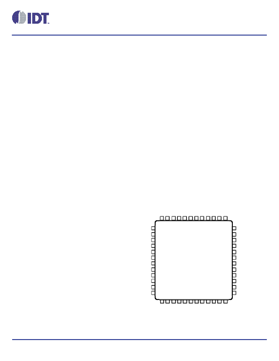
Pin Assignment
13 14 15 16 17 18 19 20 21 22 23 24
1
2
3
4
5
6
7
8
9
10
11
12
QC
48 47 46 45 44 43 42 41 40 39 38 37
V
QD0
QD1
GND
VDDO_B
QB0
VDD
nOE_D
GND
nPLL_ SEL
XTAL_IN
XTAL_OUT
nXTAL_SEL
CLK
nCLK
nOE_C
nOE_B
GND
V
DD
nO
E
_
A
nOE_REF
CORE_SEL
SP
I_
S
EL
1
SP
I_
SE
L0
DD
R
_
S
E
L
1
DD
R
_
S
E
L
0
PC
I_
S
E
L1
PC
I_
S
E
L0
V
DD
A
nLVD
S
_S
EL
48- Pin TQFP,E- Pad
7mm x 7mm x1mm
package body
Y Package
Top View
nQ
A
QA
V
DD
VDDO_B
QB1
DDO_CD
36
35
34
33
32
31
30
29
28
27
26
25
V
DD
O
_
R
E
F
nO
E
_
E
GN
D
GND
V
DD
O
_
R
E
F
QE
V
DD
O
_
E
GND
QREF2
QREF1
QREF0
ICS8430S10I-02
7mm x 7m x 1mm
package body
& Package
Top View
发布紧急采购,3分钟左右您将得到回复。
相关PDF资料
ICS84314AY-02LFT
IC SYNTHESIZER 700MHZ 32-LQFP
ICS843156AKILF
IC CLK GENERATOR 32VFQFP
ICS843156AKLF
IC CLK GENERATOR 32VFQFP
ICS843202AYILF
IC SYNTHESIZER 680MHZ 32-LQFP
ICS843204AGILF
IC SYNTHESIZER LVPECL 48-TSSOP
ICS84320AY-01LN
IC SYNTHESIZER GP LVPECL 32-LQFP
ICS84320AYI-01LF
IC FREQ SYNTHESIZER 32TQFP
ICS843251AG-04LF
IC CLK GENERATOR LVPECL 8-TSSOP
相关代理商/技术参数
ICS8430S10BYI-02LFT
功能描述:IC CLK GENERATOR PLL 48TQFP RoHS:是 类别:集成电路 (IC) >> 时钟/计时 - 专用 系列:- 标准包装:1,500 系列:- 类型:时钟缓冲器/驱动器 PLL:是 主要目的:- 输入:- 输出:- 电路数:- 比率 - 输入:输出:- 差分 - 输入:输出:- 频率 - 最大:- 电源电压:3.3V 工作温度:0°C ~ 70°C 安装类型:表面贴装 封装/外壳:28-SSOP(0.209",5.30mm 宽) 供应商设备封装:28-SSOP 包装:带卷 (TR) 其它名称:93786AFT
ICS8430S10I-03
制造商:IDT 制造商全称:Integrated Device Technology 功能描述:Clock Generator for Cavium Processors
ICS8431-01
制造商:ICS 制造商全称:ICS 功能描述:200MHZ, LOW JITTER, LVPECL FREQUENCY SYNTHESIZER
ICS843101-312
制造商:ICS 制造商全称:ICS 功能描述:FEMTOCLOCKS⑩ CRYSTAL-TO-LVPECL 312.5MHZ FREQUENCY MARGINING SYNTHESIZER
ICS843101AG-312
制造商:ICS 制造商全称:ICS 功能描述:FEMTOCLOCKS⑩ CRYSTAL-TO-LVPECL 312.5MHZ FREQUENCY MARGINING SYNTHESIZER
ICS843101AG-312LF
制造商:ICS 制造商全称:ICS 功能描述:FEMTOCLOCKS⑩ CRYSTAL-TO-LVPECL 312.5MHZ FREQUENCY MARGINING SYNTHESIZER
ICS843101AG-312LFT
制造商:ICS 制造商全称:ICS 功能描述:FEMTOCLOCKS⑩ CRYSTAL-TO-LVPECL 312.5MHZ FREQUENCY MARGINING SYNTHESIZER
ICS843101AG-312T
制造商:ICS 制造商全称:ICS 功能描述:FEMTOCLOCKS⑩ CRYSTAL-TO-LVPECL 312.5MHZ FREQUENCY MARGINING SYNTHESIZER